UCLA-led research team produces most accurate 3D images of ‘2D materials’

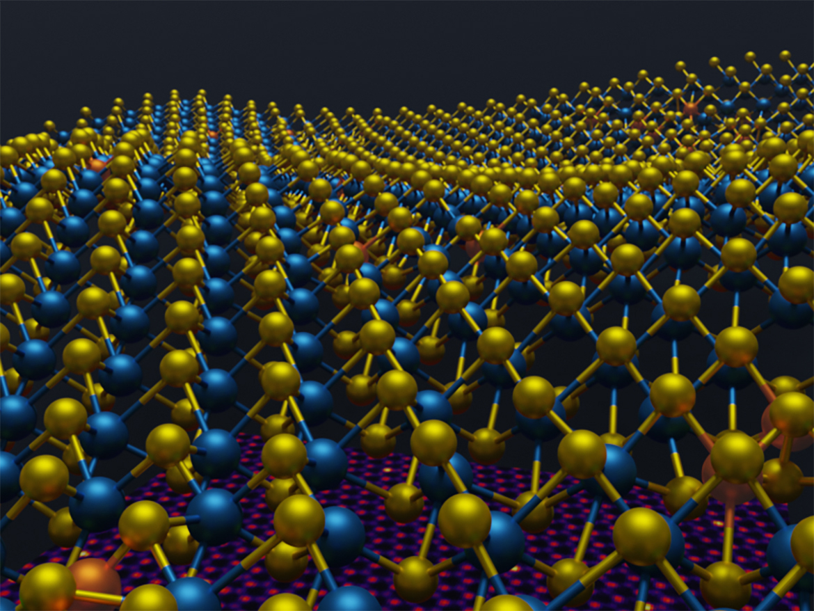
Image showing the 3D atomic coordinates of molybdenum (blue), sulfur (yellow) and added rhenium (orange). A 2D image is shown beneath the 3D model. (Photo Credit: Dennis Kim/UCLA)
A UCLA-led research team has produced in unprecedented detail experimental three-dimensional maps of the atoms in a so-called 2D material — matter that isn’t truly two-dimensional but is nearly flat because it’s arranged in extremely thin layers, no more than a few atoms thick.
Although 2D-materials–based technologies have not yet been widely used in commercial applications, the materials have been the subject of considerable research interest. In the future, they could be the basis for semiconductors in ever smaller electronics, quantum computer components, more-efficient batteries, or filters capable of extracting freshwater from saltwater.
The promise of 2D materials comes from certain properties that differ from how the same elements or compounds behave when they appear in greater quantities. Those unique characteristics are influenced by quantum effects — phenomena occurring at extremely small scales that are fundamentally different from the classical physics seen at larger scales. For instance, when carbon is arranged in an atomically thin layer to form 2D graphene, it is stronger than steel, conducts heat better than any other known material, and has almost zero electrical resistance.
But using 2D materials in real-world applications would require a greater understanding of their properties, and the ability to control those properties. The new study, which was published in Nature Materials, could be a step forward in that effort.
The researchers showed that their 3D maps of the material’s atomic structure are precise to the picometer scale — measured in one-trillionths of a meter. They used their measurements to quantify defects in the 2D material, which can affect their electronic properties, as well as to accurately assess those electronic properties.
“What’s unique about this research is that we determine the coordinates of individual atoms in three dimensions without using any pre-existing models,” said corresponding author Jianwei “John” Miao, a UCLA professor of physics and astronomy. “And our method can be used for all kinds of 2D materials.”
Miao is the deputy director of the STROBE National Science Foundation Science and Technology Center and a member of the California NanoSystems Institute at UCLA. His UCLA lab collaborated on the study with researchers from Harvard University, Oak Ridge National Laboratory and Rice University.
The researchers examined a single layer of molybdenum disulfide, a frequently studied 2D material. In bulk, this compound is used as a lubricant. As a 2D material, it has electronic properties that suggest it could be employed in next-generation semiconductor electronics. The samples being studied were “doped” with traces of rhenium, a metal that adds spare electrons when replacing molybdenum. That kind of doping is often used to produce components for computers and electronics because it helps facilitate the flow of electrons in semiconductor devices.
To analyze the 2D material, the researchers used a new technology they developed based on scanning transmission electron microscopy, which produces images by measuring scattered electrons beamed through thin samples. Miao’s team devised a technique called scanning atomic electron tomography, which produces 3D images by capturing a sample at multiple angles as it rotates.
The scientists had to avoid one major challenge to produce the images: 2D materials can be damaged by too much exposure to electrons. So for each sample, the researchers reconstructed images section by section and then stitched them together to form a single 3D image — allowing them to use fewer scans and thus a lower dose of electrons than if they had imaged the entire sample at once.
The two samples each measured 6 nanometers by 6 nanometers, and each of the smaller sections measured about 1 nanometer by 1 nanometer. (A nanometer is one-billionth of a meter.)
The resulting images enabled the researchers to inspect the samples’ 3D structure to a precision of 4 picometers in the case of molybdenum atoms — 26 times smaller than the diameter of a hydrogen atom. That level of precision enabled them to measure ripples, strain distorting the shape of the material, and variations in the size of chemical bonds, all changes caused by the added rhenium — marking the most accurate measurement ever of those characteristics in a 2D material.
“If we just assume that introducing the dopant is a simple substitution, we wouldn’t expect large strains,” said Xuezeng Tian, the paper’s co-first author and a UCLA postdoctoral scholar. “But what we have observed is more complicated than previous experiments have shown.”
The scientists found that the largest changes occurred in the smallest dimension of the 2D material, its three-atom-tall height. It took as little as a single rhenium atom to introduce such local distortion.
► Read a Nature analysis of the UCLA-led study
Armed with information about the material’s 3D coordinates, scientists at Harvard led by Professor Prineha Narang performed quantum mechanical calculations of the material’s electronic properties.
“These atomic-scale experiments have given us a new lens into how 2D materials behave and how they should be treated in calculations, and they could be a game changer for new quantum technologies,” Narang said.
Without access to the sort of measurements generated in the study, such quantum mechanical calculations conventionally have been based on a theoretical model system that is expected at a temperature of absolute zero.
The study indicated that the measured 3D coordinates led to more accurate calculations of the 2D material’s electronic properties.
“Our work could transform quantum mechanical calculations by using experimental 3D atomic coordinates as direct input,” said UCLA postdoctoral scholar Dennis Kim, a co-first author of the study. “This approach should enable material engineers to better predict and discover new physical, chemical and electronic properties of 2D materials at the single-atom level.”
Other authors were Yongsoo Yang, Yao Yang and Yakun Yuan of UCLA; Shize Yang and Juan-Carlos Idrobo of Oak Ridge National Laboratory; Christopher Ciccarino and Blake Duschatko of Harvard; and Yongji Gong and Pulickel Ajayan of Rice.
The research was supported by the U.S. Department of Energy, the U.S. Army Research Office, and STROBE National Science Foundation Science and Technology Center. The scanning transmission electron microscopy experiments were conducted at the Center for Nanophase Materials Sciences, a DOE user facility at Oak Ridge National Laboratory.
This article originally appeared in the UCLA Newsroom.


